Hamed Sadeghian: A trailblazer in the semiconductor industry
The 10 Most Innovative Business Leaders to Follow in 2021
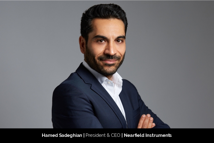
An exceptionally bright and motivated
leader, Hamed Sadeghian, CEO of Nearfield Instruments, is pushing the borders
between disciplines, science and business to create innovative and better
solutions in the semiconductor industry.
He believes that premium electronics play a
crucial role in the modern world. Modern technologies like mobile
communication, cloud computing, Big Data, blockchain, and IoT have the power to
cause rapid advancements and transform the whole world industry, leading to
Artificial intelligent of things. He aims to harness the power of these
technologies and shape the world atom by atom.
Rise of a mature leader
Hamed started his Bachelor of Science (BSc)
in Mechanical Engineering in 2000 at Isfahan University of Technology. The next
year, in 2001, he joined forces with Machine Ajza Co. He was a Mechatronics
Systems Engineer and was responsible for realizing Mechanical and Mechatronics
Equipment for Oil and Gas industry, Steel production industry, and Gas turbine
Industry, including design, manufacturing, assembly, installation, FAT &
SAT. Moreover, he was responsible for DFX of all equipment development and
technology groups with 10 FTE. While working, he also co-founded Jahesh Poulad
Co. and became the CTO of the company. Here he took the onus for the
responsibilities of a Systems Engineer. Besides this, he was responsible for
acquiring projects and defining concepts with customers for mechanical
equipment, being used in the high volume production of Steel Industry, Oil
& Gas & Transportation industry.
After finishing his MSc in Mechanical
engineering and selling his company, Jahesh Poulad, In 2007, he started his
Doctor of Philosophy in Mechanical Engineering from the Delft University of
Technology and completed it with Cum Laude status. After completing his PhD, he
became a Postdoctoral Researcher and then Senior Researcher at TU Delft. He
supervised MSc and PhD students, conducted research in the field of Nano-Optomechatronics
instruments, and wrote research proposals for National, European, and
International funding agencies.
While taking charge as senior researcher,
he joined forces with TNO as the Senior System Architect. He was the System
Architect of Optomechatronics Instruments and equipment, including metrology,
inspection, and characterization systems for semiconductor and bio-medical
applications. In 2015, Hamed became the Principal Scientist and group leader of
NOMI.
In 2014, he completed his Master of Business
Administration (MBA) in Executive MBA-Innovation Management, Entrepreneurship
from the Vlerick Business School in Belgium.
Having been operating in the semiconductor
industry since 2011, he took a deep dive into the industry in 2016 and founded
Nearfield Instruments. He adds, “What I love about the semiconductor industry
is that it moves the technology forward. The semiconductor industry is the true
enabler of trends such as AI, 5G in the data era.”
He believes that creating something new is
never easy. He stresses the point by adding the quote of Peter Thiel(Founder
and CEO of Paypal), “It is much harder to make something new than to copy a
model.”
Moreover, he knows that timing plays a
vital role while launching a business in the market. He adds, “It is all about
the right timing. Understanding the market we are in, we were able to assess if
the timing is right. It is important not to start the business in a market
(segment) with many big players. I prefer starting a business in a rather
smaller market with a bigger share of our product.”
He further adds, “We will be part of the AI
devices you will use in near future. Our process control solutions is essential
and reliable in producing semiconductor chips. It will contribute to enable the
world’s top chipmakers to create better performing, cheaper chips. As chips
advance, more tasks that used to be sent to remote computer servers for
processing can be done locally. We’ve already seen smartphones become capable
of transcribing voice notes and recognizing people in photos without the need
for an internet connection. Now even more complex “artificial intelligence”
jobs become possible, potentially helping smartphones make better sense of the
world around them.”
Getting stronger with the challenges
Hamed believes that challenges play a key
role while climbing the ladder of success. They groom one’s perspective and
allow one to evolve into a stronger personality. However, the prime thing is to
take them as learning lessons without being a victim.
In the journey to take the company to the
next level, Hamed Faced several challenges. First, he had to convince customers
that their solution is unique and disruptive compared to the competition. They
also needed to secure funding, and the semiconductor industry is very capital
intensive, with very high risk. It is not like a software development company,
where risks are considerably lower and required working capital are minute
compared to DeepTech like Nearfield Instruments, where they develop and build
one of the most complex machines ever made by humankind. At last, he had
to attract top talent and retain them, scale up the organization, shape the
culture of the company and its core values. Hamed never gave up and tunneled
through all the challenges to pave the company to the top.
Offering innovative solutions with
Nearfield Instruments
Nearfield Instruments is a DeepTech
scale-up active in the semiconductor industry. The company operates from
Rotterdam (head office), Eindhoven (High Tech Campus), and South Korea. Currently,
it employs 110 employees.
The company develops and delivers
ground-breaking process control metrology solutions that are able to measure
essential 3D nanostructures in a non-destructive manner during the
manufacturing process of microchips. Examples of microchips are memory and
logic processors for laptops, smartphones, data centers, Automotive, etc.
Measuring these structures is essential to be able to produce high performance
chips.
Nearfield Instruments’ customers are global
microchip manufacturers. Hamed adds, “The technique developed by Nearfield
Instruments is based on so-called “Scanning Probe Microscopy” (SPM), which
scans the surface in three dimensions with an atomically sharp tip. Nearfield
Instruments has improved and refined SPM to achieve significant measurement
speeds and non-destructively measure complex 3D structures, both on the surface
and below the surface. Other metrology technologies (which often work based on
electrons or light (photons)) cannot measure the very smallest 3D nanostructures
precisely or quickly enough non-destructively.”
Nearfield Instruments is uniquely
positioned and has the ambition to grow into a world-leading semiconductor
metrology equipment supplier. Nearfield Instruments cooperates closely with the
excellently developed high-tech ecosystem in the Netherlands.
Revamping the Semiconductors Industry
With electronics becoming a crucial part of
everyone’s lives, it has become significantly important to adopt new
technologies and embrace the new transformation. Numerous technologies such as
Big Data, cloud computing as well as mobile communication are all based on
consistently advancing electronics and their core technology, namely,
integrated circuits (IC) or chips.
Although from past years, the chips or
semiconductor industry has been driven by tablets, smartphones, servers, and
PCs, now fast-pacing AIoT is also witnessing its taste. Till now, chip
manufacturers have been pushing their limits to add new functionalities and
applications. However, now they have finally found their new companions in
wearable electronics (e.g., for health applications), the Internet of Things
(IoT), artificial intelligence (AI; e.g., for societal challenges such as
climate change), and advanced driver assistant systems (ADAS; e.g., for
enhancing smart mobility).
He adds, “The semiconductor industry has
marched at the pace of Moore’s Law for a long time that is transistor scaling
associated with doubling the computing power of a chip every two years, whereas
simultaneously chips have become more energy efficient. However, recent growth
is scaling up the demand for novel semiconductor manufacturing and metrology
processes. The demand for even more powerful and lower-power-consuming
electronics at constant pricing levels has never been so high. Two-dimensional
(2D) transistors following the traditional Moore’s Law are, however, not
capable of satisfying these demands.”
Thus, to get chips with exceptional
performance, IC devices need to shrink to highly small dimensions, that is,
atomic-scale dimensions. This is possible using novel, complex designs with
high-aspect ratios (HARs), sensitive materials, and 3D structures. Named as
subsurface features, these structures are known to have logic features that are
buried under a significant number of layers (> 100 nm).
Engineers stack different Nanowires or
nanolayers on top of each other below a plethora of metal and gate layers,
whereas in 3D NAND, different memory features are properly positioned in these
layered devices. Also, they come with about 170 layers nowadays and will only
increase in the upcoming future (till 512 layers). Most of these layers are
composed of metal or poly layers that are fully optically non-transparent
(opaque). The production of 3D semiconductor device architectures helps in
augmenting the chip performance and, at the same time, costs significantly
lower.
He adds, “As in every manufacturing
process, there is a famous adage in semiconductor IC manufacturing, “if you
cannot measure it, you cannot make it.” To produce a nano-architecture in a
technologically and economically viable way, the need for neat control over the
manufacturing process is key. Film quality (thickness, material properties,
uniformity), feature quality (linewidths, edge profiles, uniformity), and low
device defect density (voids, impurities, contaminations) must be preserved
within very tight limits. To reach a maximum yield of next-generation IC
devices in new manufacturing processes, breakthroughs in metrology are
required, which is the science of measuring and characterizing tiny structures
and materials.”
Semiconductor manufacturing process
Each semiconductor includes about 80 to 100
cycles for realizing layer-by-layer growth, and each cycle consists of 5
process steps. Previously, metrology was applied after every cycle (step 5) for
addressing defects in the produced layer(s). The Next-generation metrology
needs some features. Explaining those features in detail, he states, “Firstly,
Critical Dimensions (CD) of (subsurface) features and wafer surface roughness
need to be measured down to sub-nanometre level (known as CD Metrology).
Secondly, critical (subsurface) defects need to be imaged and measured in three
dimensions to trace back their origin without affecting the wafer quality
(Defect Review). Thirdly, with the full switch to 3D features produced by
extreme ultraviolet lithography (EUV), the alignment of different IC layers
known as ‘overlay’ requires atomic-scale precision (< 1 nm) in positioning
and monitoring (Overlay Metrology; see below).”
All the above-mentioned precision
requirements need to be fulfilled with higher throughput, increased pressure
for automation, no tolerance for destructivity on the wafers, as well as
increased long-term reliability for decreased prices.
Overlay Metrology
Hamed further shares more about the crucial
metrology applications of the new 3D devices, which is overlay metrology. For
brilliant device performance and great yield of manufacturing, the overlay
(layer-to-layer misalignment) must be less than 1 nm.
Sharing more about this in detail, he says,
“Optical solutions require the use of optical test targets, often very big,
located in the scribe lines of the chips to measure the overlay between the top
layer under process and the previous, subsurface layers. In the presence of
opaque layers, photons cannot penetrate these layers. Thus optical solutions do
not work. Another issue with measuring overlay via these (remote) targets is
that it does not represent the real (local) overlay values on the devices for
nodes < 10 nm. Therefore, the industry is moving in the direction of
measuring the overlay on the device itself, rather than using targets.”
For manufacturing novel 3D devices with
excellent subsurface features and following all the metrology precision
requirements as stated above, Nearfield Instruments develops innovative
Subsurface Scanning Probe Microscopy (SSPM) solution, which is the world’s 1st
non-destructive and subsurface 3D metrology system for enabling Subsurface CD,
Subsurface Defect Review, and Overlay Metrology.
Flourishing Ahead
Nearfield Instruments (NFI) has recently
received significant investments of €12 million (from existing shareholders
Eugene Investment & Securities, a Korean financial services firm) and €17.5
million (€ 10,5 million from Dutch impact investor Invest-NL and € 7
million from another existing shareholder Innovation Industries). They have
also signed a memorandum of understanding with VDL ETG to further strengthen
their long-term strategic partnership as well as establish a Korean subsidiary
in Hwaseong and plan to expand their footprint even further than this with new
subsidiaries and strategic partnerships.


